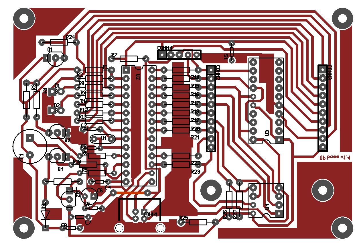
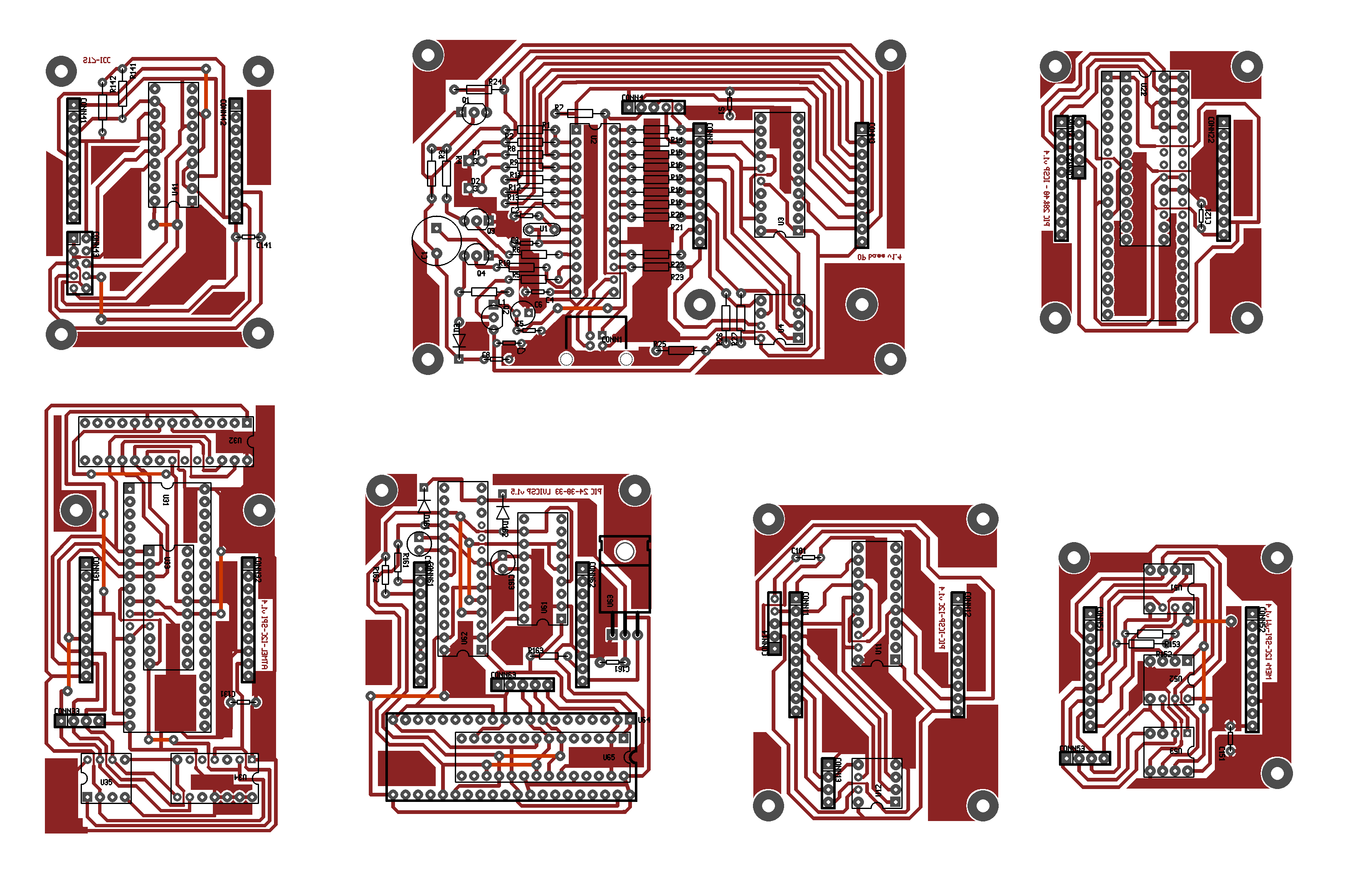
Many components are optional, are only needed to program some types of devices or for future applications: expansion connectors CONN2-3, protection resistors R11:23 (considering their cost why not use them?), I2C pull-up resistors R26-27, S1 switch, ICSP-IN CONN4 (right now it's used to program the main microcontroller without extracting it).
The pcb was optimized to fit the solder side, however a few jumpers are needed on the component side; if you want you can avoid that by using a double side pcb.
Pay attention to the orientation of transistors: Q1's emitter to the left, Q2 up, Q3 and Q4 right.
Once connected to the PC, a working circuit blinks D2 at 4Hz until the enumeration is completed, then at 1Hz.
To verify that everything is working correctly use the "Hardware Test" function in the control program: in this mode, to be executed without target devices, all the outputs (CK, D, PGM, VDDU, VPPU, which can be reached on pins 14-15-12-1-4 of U3, with respect to GND, pin 5) are activated in various combinations; if the measured voltages correspond to what is presented on screen then the hardware is correctly assembled.
VPP voltage could be different from the set value by up to 1V; this is due to the fact that the DCDC converter takes VCC as reference voltage; the latter comes from the USB cable and can vary from 4.75V to 5.25V; in addition the feedback voltage divider (R1-R2) can introduce another 5% of error.
The most common causes of malfunction are:
incorrect orientation of transistors,
incorrect inductor value,
pcb defects like shorts or opens,
unsoldered capacitors,
main microcontrollorer not programmed.
Component list:
U1 12Mhz quartz (also 4, 8, 16, 20; reconfiguration of input divider options is required)
U2 18F2550 (also 2450,2455,2458,2553,4450,4455,4458,4550,4553)
U3 20p socket.
U4 8p socket.
Q1-2 BC557 (or any PNP, pay attention to polarity)
Q3-4 BC547 (or any NPN, pay attention to polarity)
D1-2 LED
D3 1N4148 (or any diode, better if Shottky)
L1 100uH resistor type or other
R1 22K
R2 12K
R3 100K
R4:6 10K
R7 1M
R8-9 2.2K
R10 10K
R11:23 100
R24-25 300K
R26-27 10K
C1 22-100uF 25V
C2-3 22pF
C4 >= 220nF
C5 100nF
C6 10uF
C7-8 100nF
CONN1 USB type B
CONN2-3 10 pin female stripline
CONN4 5 pin stripline
How to use
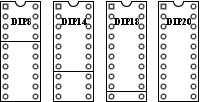
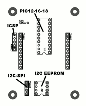
The basic circuit can host PIC devices with 8, 14, 18, and 20 pins (except 10Fxxx); they should be inserted in U3 with alignment to pin1:
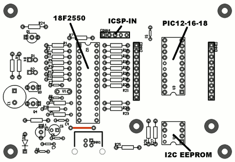
I2C memories go in U4.
I plan to make an adapter for 10Fxxx with 6 or 8 pins; in the meantime it's possible to get by using wires.
Other devices can be programmed using expansion boards plugged to connectors CONN2-3:
- 28-40 pin PICs + ICSP connector
- 8-20 pin PICs (same as main board, but there's more space for a ZIF socket) + ICSP conn.
- 3.3V PIC16-18 + ICSP conn. (this board has also a 3.3V regulator)
- PIC24-30-33 + ICSP conn. (this board has also a 3.3V regulator)
- I2C, SPI, uW memories and I2C-SPI conn.
- 8-14-20-28-40 pin ATMEL micros and I2C-SPI conn
- ST72 (future)
Of course they're not required for basic operation.
In assembling the adapters I suggest to insert the expansion connectors from the component side, and keep their plastic spacer on that side; this improves the solder strength, especially during extraction.
In case of 3.3V devices the presence of a 3.3V adapter (which has RB1 and RB0 shorted) is checked by the software in order to avoid irreversible damage.
The 16F1xxx could be programmed also without such adapter (only the 16LF1xxx need it), but the check is present for both so there is no chance of confusion.
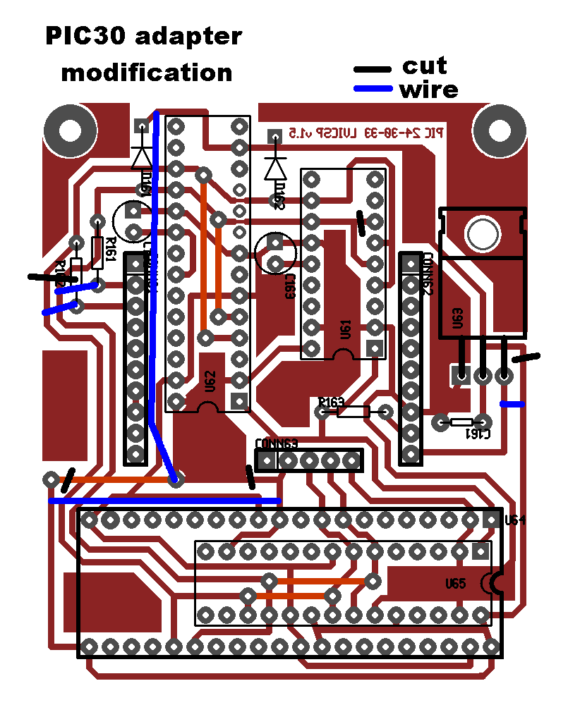
Due to the impossibility of erasing dsPIC30 protection registers at 3.3V, these devices are now powered at 5V; who already made the adapter (prior to v. 1.7) can easily
modify it.
The following images show how to insert various target devices in the expansion boards:
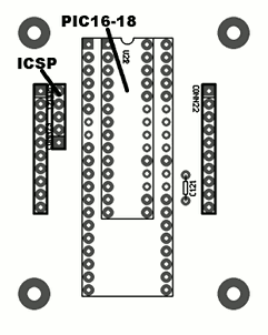

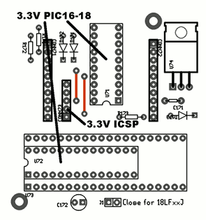
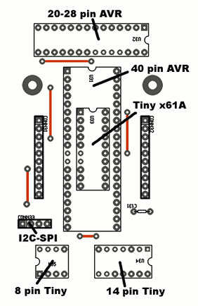
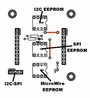
Smaller devices have to be aligned to pin 1 of the respective socket.
Target chips can also be programmed in circuit by routing ICSP signals (VPPU,VDDU,ICD,ICK,GND) to the application board; these signals are present in the base module expansion connectors or in some expansion boards as a discrete connector; note that low voltage devices require ICSP signals from a low voltage expansion board.
ICSP-IN connector is used to program the main micro without extracting it, by means of another programmer.
Pin mapping of various connectors in the base and expansion boards:
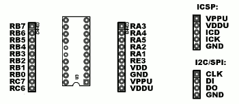
Map of resources used:
| Pin | Various functions | ICSP | I2C-EEPROM | SPI-EEPROM | SPI-ATMEL | uW-EEPROM |
| RB7 | | PGM | | | | |
| RB6 | | ICSP clock | | | | |
| RB5 | | ICSP data | A2 | | | W (6) |
| RB4 | | | A1 | HLD | | S (1) |
| RB3 | | | A0 | CS | Device clock | PRE (7) |
| RB2 | expansion | | | | | |
| RB1 | | | Clock | Clock | SPI Clock | Clock |
| RB0 | | | Data | Data out (MOSI) | Data out (MOSI) | Data out |
| RC7 | | | | Data in (MISO) | Data in (MISO) | Data in |
| RC6 | | | WP | WP | RESET | |
| RC5 | USB D+ | | | | | |
| RC4 | USB D- | | | | | |
| RC2 | DCDC PWM | | | | | |
| RC1 | controls VDD | | | | | |
| RC0 | controls VPP | | | | | |
| RA5 | expansion | | | | | |
| RA4 | expansion | | | | | |
| RA3 | expansion | | | | | |
| RA2 | LED 2 | | | | | |
| RA1 | LED 1 | | | | | |
| RA0 | ADC for
regulator | | | | | |
| RE3 | S1 switch | | | | | |
The schematic diagram was drawn with Gschem, an open source program that comes with
GEDA suite.
In their website it's not evident (as they all use linux), but it's also possible to run the program in windows under
cygwin; I suggest to use the latest version (you need to compile sources).
PCBs were drawn with
PCB; in this case there is also a (somewhat limited) windows version.
With a little effort the circuit can also be mounted on experimental boards, without pcb.
Schematic diagram of base module:
.pdf,
.png; expansion boards:
.pdf; everything in gschem format:
Oprog.sch
Pcb of base module:
.pdf,
.png; base module + expansion boards:
.pdf,
.png; everything in PCB format:
Oprog.pcb
Complete archive, includes sources, gerber, pdf, png
How to program the main micro the first time?
This is an interesting problem: a new device can't work as programmer, so it must be programmed in some way.
Apart from asking someone else to do it for you, my advice is to build one of those serial programmers, like JDM, to do the job the first time.
It may seem strange to use a programmer to build another one, but there is no way to interface USB without firmware; I think the effort is worth it because serial programmers are not very reliable, are slow, and of course not portable to new computers that lack serial ports.
It would also be a good idea to buy a backup micro, in order to program it with updated firmware versions.
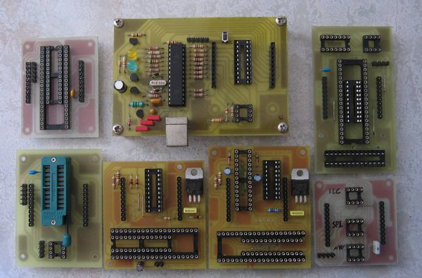
The main circuit and some expansion boards (28-40p PIC, 8-20p PIC with ZIF, 3.3V PIC16-18, 3.3V PIC24-30-33, EEPROM, ATMEL):
Switching voltage regulator
In order to generate a voltage higher than 5V we need a boost switching converter.
On the market there are thousands of single chip solutions, but I used instead the microcontroller itself and a few external components.
The width of output pulses will vary to keep the output voltage stable over all operating conditions.
In practice this is a digitally controlled regulator, as shown in the following diagram:
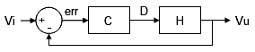
The ADC converter presently uses the 5V supply as a reference, so the output voltage will follow it; it is possible to connect an external reference to RA3 to improve the overall precision.
Switching frequency is 90 kHz, which is well over the cutoff frequency of the output LC filter (~2,3 kHz).
The performance is limited by losses due to the transistor, diode, inductor, but since the load is very low we can use low-cost (even recycled) components; to improve load capability switch to a better transistor, a Shottky diode, a higher rated inductor.
Anyways, in order to design a suitable regulator (block C above) it's necessary to work in s domain and model the converter itself; this has fortunately been done already, some info is available for example
here.
With present component values the boost converter operates in dicontinuous mode; critical current is:
Icrit=Vu*T/(16*L)=86 mA
well over expected load, supposed to be 1 mA.
Other parameters:
Vi=5
Vu=12.5
D=(Vu-Vi)/Vo
L=100e-6
C=47e-6
I=1e-3
R=12/I
Rl=1.6 (inductor series resistance)
T=1/90e3
vu 1 vu M-1 Vu 2M -1
--- = Gdo ---------- where Gdo = 2 --- ------- , M = ---, wp = ----------
D 1 + s/wp D 2M -1 Vi (M-1) RC
Transfer function results to be:
vu 127.58
-- = -------------
D 0.22031 s + 1
Which has the following Bode diagram:
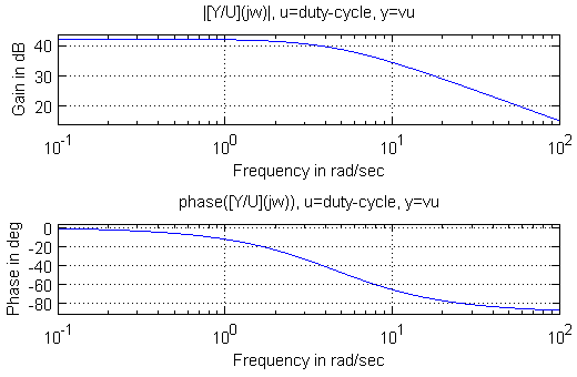
It seems that the system, in closed loop, would be stable even by itself; however it would have a steady state error of 1/DCgain.
It's better to use a controller with a pole on the origin and a zero to stabilize everything, for example the following controller:
D 0.25 (s + 50)
C = --- = -------------
err s
Overall transfer function would be:
vu 144.77 s + 7238.4
-- = -----------------
vi s2 + 4.539 s
The system is stable, with a phase margin of ~75º.
Since we operate in the digital domain we must choose the sampling frequency.
It can't be too high because of execution speed; if too low it limits the regulator bandwidth; a period of 250 us was a good compromise.
The various transfer functions are converted to z domain using bilinear transformation:
vu 0.018199 z2+ 0.00022607 z - 0.017973
-- = ------------------------------------
vi z2 - 1.9989 z + 0.99887
The controller is:
D 0.25156*z - 0.24844 C1 - C2 z-1
C = --- = ------------------- = -----------
err z - 1 1 -z-1
Remember that z
-1 represents a delay of one clock cycle.
Next we must deal with quantization and calculation errors.
A/D converter is 10 bits wide, and is triggered by timer2; at the end of conversion an interrupt calls the regulation routine, which calculates the new duty cycle for the PWM peripheral, also 10 bits wide.
On the feedback path it's necessary to include a voltage divider in order to limit ADC input voltage to [0,5V]; R1 and R2 do this.
So the block diagram is modified as follows:
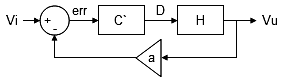
a=12/34
Vu=C'H(Vi-aVu)
Vu C'H
-- = ------
Vi 1+aC'H
To compare with the previous model we can multiply both terms by a; simply remembering to change the set point we can decide that the new input is Vi/a, and equate with the previous expression:
Vu aC'H CH
---- = ------ = ----
Vi/a 1+aC'H 1+CH
aC'=C
aC1' - aC2' z-1 C1 - C2 z-1
aC'= --------------- = C = ------------
1 - z-1 1 - z-1
aC1'=C1
aC2'=C2
Since the hardware works with 10 bit digital data we can go from D/err to pwm/[err]:
[err]=err*1024/5
pwm=D*1024
D pwm/1024 pwm C1' - C2'z-1
C'= --- = ------------ = ------- = ------------
err [err]/1024*5 [err]*5 1 -z-1
pwm(1 - z
-1)=[err](5*C1/a - 5*C2/a z
-1)=[err](3.564 - 3.52 z
-1)
It's clear that integer multiplications can't be used with these coefficients; the easiest solution is to work with fractional values (i.e. divide output by 2
N and multiply coefficients accordingly); considering that pwm output is 10 bits wide and left-aligned, we can easily work with values divided by 64.
pwm(1 - z
-1)=[err](k1 - k2 z
-1)/64
k1=5C1/a*64=228.12 ~ 228
k2=5C2/a*64=225.25 ~ 225
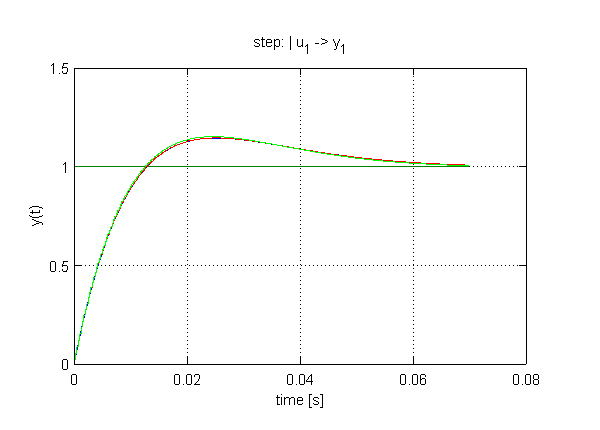
Following are step responses of continuous-time system (blue), discrete-time system (red), discrete-time system with approximate cefficients (green); As you can see they're almost coincident.
For all calculations I used
Octave, an open source mathematical modeling tool; version 3 has just been released, and it can be used also under the famous windows (almost)operating system.
If someone is interested
these are the modeling scripts I used.
The real code for the control function was written in assembly; this is necessary for performance reasons.
In fact our C compiler calls a library function to perform multiplications, so it has to save many variables on the stack causing a delay; in this case the resulting execution time had reached 50 us, which is a significant fraction of the sampling period.
Instead, by avoiding function calls and manually coding the 16x8 bit multiplication (see k1 & k2), the execution time is down to 12 us.
Some real waveforms:
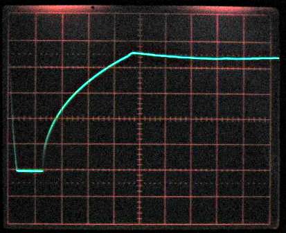
Power-up transient, 50 ms/div
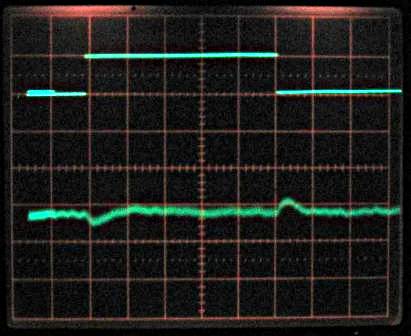
Step response to load change (load on top trace, AC coupled output on bottom tr.), 50ms/div
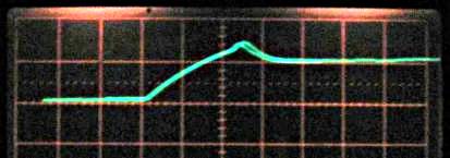
Step response to set point change (from 11,5 to 12,5 V), 50 ms/div
How to contribute
The best way to contribute to this project is to build it, use it, and report bugs or suggestions.
Also there are still many devices to test; check the list in
supported devices.
Whoever has the know-how and patience can also expand support to other devices.
Or if you have a device that is not supported you can send it to me so that I can work on it.
If you find this project useful write me a couple of lines:

, and if you modified it show me your work.
On SourceForge you can find some
forums where you can discuss about this project.
Downloads
Schematic diagram and pcb:
complete archive.
Firmware:
complete MPLAB project or
compiled firmware (.hex) or
a version for 18F2450 (with reduced functionality, see
the circuit).
OP (command-line for Linux & Windows)
OpenProg (windows):
application only;
sources (Visual Studio 6 workspace)
opgui (GTK GUI for Linux & Windows)
Octave scripts
History
| a long time ago | need for a reliable and free USB programmer |
| 2007 | experiments with USB PIC and varionus firmwares; voltage regulator |
| 2008 | first prototypes and software |
| july 2008 | documentation and website, released version 0.3 |
| august 2008 | version 0.4: added support for I2C EEPROMs |
| november 2008 | version 0.5: I2C & SPI bus, added some ATMEL devices |
| january 2009 | control progs v0.5.1: added some PIC devices, removed some bugs |
| march 2009 | control progs v0.5.2 and v0.5.3: added some PIC an Atmel devices, removed some bugs |
| april 2009 | schematic diagram and pcb v1.4: changed Atmel adapter |
| june 2009 | version 0.6: fully GPL2 USB firmware, added 93Sx6 MicroWire EEPROMs |
| september 2009 | version 0.6.1: solved some SPI bugs, added some Atmel devices and 93Cx6C |
| october 2009 | control progs v0.6.2: bugfix |
| january 2010 | version 0.7.0: added PIC24 and SPI EEPROMs;
circuits v1.5: expansion board for 3.3V PIC24-30-33 |
| february 2010 | control progs v0.7.1: added some PIC18 and Atmel devices; bugfix |
| march 2010 | control progs v0.7.2: added some MicroWire eeproms; bugfix |
| april 2010 | control progs v0.7.3: added PIC16F1xxx; OP works in windows; code rework and bugfix;
circuits v1.6: expansion board for 3.3V PIC16-18 |
| may 2010 | control progs v0.7.4: added PIC18FxJx, PIC18FxKx, PIC24H, dsPIC30-33, ATtiny2313, 241024; bugfix;
circuits v1.7: modified PIC24-30-33 expansion board, PIC30 now at 5V |
| june 2010 | control progs v0.7.5: corrected write bug for 18Fx config, added "goto ICD" write for 16Fx, various minor fixes |
| july 2010 | firmware v0.7.6: modified TX16 and RX16 with variable period for communication with ICD;
control progs v0.7.6: byte by byte read with 93xx6 for better compatibility;
first release of pdb debugger (v0.1); |
| august 2010 | control progs v0.7.7: added 16F72x, some minor fixes;
circuits v1.7.1: reduced value of R173 on the PIC16/18 LV expansion board |
| april 2011 | control progs v0.7.8: updated algorithms for 16F87xA and 16F62xA,
16F1822 becomes 12F1822, added 30F1010, 30F2020, 30F2023, 16F1847, 12F1840 16F1516, 16F1517, 16F1518, 16F1519, 16F1526, 16F1527;
greater modularity for source code, corrcted some bugs |
| june 2011 | control progs v0.7.9: added ATtiny11-12-24-26-261-44-48-461-4313-84-88-861, ATmega48-88-164A-168-324A-328-644A-1284, 16LF1902-3-4-6-7, various minor modifications and fixes;
new graphical interface based on GTK for Linux and Windows |
| the future | increase support for PIC and ATMEL micros (as soon as I can get free samples); add ST72, JTAG, parallel memories; expand ICD support; compile firmware also with SDCC |